Logic Families: TTL and CMOS
Expert Answer & Key Takeaways
Deep dive into digital logic families, covering TTL and CMOS technologies, propagation delay, fan-out, and power dissipation.
Logic Families: TTL and CMOS
While Boolean algebra and Karnaugh maps provide the mathematical foundation for digital design, Logic Families refer to the actual physical semiconductor technologies used to build integrated circuits (ICs). A logic family is a set of compatible logic gates manufactured using a specific type of electronic circuitry.
Logic families are broadly classified into two categories based on the type of semiconductor elements used:
- Bipolar Logic Families: Use Bipolar Junction Transistors (BJTs). Examples: TTL (Transistor-Transistor Logic), ECL (Emitter-Coupled Logic).
- Unipolar Logic Families: Use Field-Effect Transistors (FETs). Examples: PMOS, NMOS, and CMOS (Complementary Metal-Oxide Semiconductor).
1. Key Performance Characteristics
To evaluate and compare different logic families (which is a core focus in GATE/UGC-NET), we analyze several critical electrical parameters.
1.1 Propagation Delay ()
Propagation delay is the time required for a signal to pass through a gate. It is the time difference between the input changing state and the output responding. It determines the maximum operating speed (frequency) of the circuit.
- Measured in nanoseconds (ns) or picoseconds (ps).
- Formula: (where is High-to-Low delay, and is Low-to-High delay).
1.2 Power Dissipation ()
The electrical power consumed by the gate, usually expressed in milliwatts (mW) or microwatts (µW). Power dissipation occurs statically (leakage current) and dynamically (during switching).
1.3 Figure of Merit (Speed-Power Product)
An ideal logic gate would be infinitely fast and consume zero power. In reality, there is a trade-off: faster gates consume more power. The Figure of Merit (SPP) evaluates this trade-off.
- Formula:
- Measured in picojoules (pJ). A lower value indicates a better, more efficient logic family.
1.4 Fan-in and Fan-out
- Fan-in: The maximum number of inputs a specific logic gate can accommodate.
- Fan-out: The maximum number of standard inputs of the same logic family that the output of a single gate can drive reliably without voltage degradation.
1.5 Noise Margin
Noise margin is the maximum noise voltage that can be superimposed on a logic signal without causing the gate to misinterpret it (e.g., mistaking a Logic 0 for a Logic 1).
- High Noise Margin:
- Low Noise Margin:
2. Transistor-Transistor Logic (TTL)
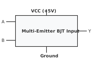
Introduced in 1964 by Texas Instruments (the 7400 series), TTL became the absolute standard for digital systems for decades. It utilizes Bipolar Junction Transistors (BJTs) to perform both the logic function and the amplifying function.
2.1 TTL Characteristics
- Supply Voltage (): Strictly (nominally). Logic 1 is typically , and Logic 0 is .
- Input Stage: Uses a unique multi-emitter transistor.
- Output Stage: Often uses a "Totem-Pole" output to provide active pull-up and pull-down, drastically reducing propagation delay.
2.2 Advantages and Disadvantages of TTL
Advantages:
- Very fast switching speeds compared to early MOS families.
- Highly robust against electrical noise and electrostatic discharge (ESD). Disadvantages:
- High continuous static power dissipation (transistors constantly draw base current).
- Lower packaging density on silicon compared to unipolar devices.
3. Complementary Metal-Oxide Semiconductor (CMOS)
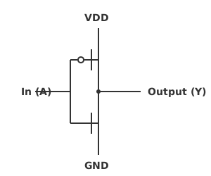
CMOS is the reigning champion of modern digital ICs, powering everything from microprocessors to smartphone SoCs. The "Complementary" refers to the fact that it uses paired, symmetrical arrays of both P-type (PMOS) and N-type (NMOS) MOSFETs.
3.1 CMOS Operating Principle
In a CMOS circuit, the PMOS transistors form the pull-up network (connecting output to ), and the NMOS transistors form the pull-down network (connecting output to Ground). Because they are complementary, when one network is ON, the other is completely OFF.
3.2 Advantages and Disadvantages of CMOS
Advantages:
- Zero Static Power Dissipation: Because there is never a direct path from to Ground in a steady state, CMOS consumes practically zero power unless it is actively switching (dynamic power).
- Excellent Noise Margin (typically of ).
- Can operate over a wide voltage range (typically to ).
- Extremely high packaging density (millions of transistors per square millimeter). Disadvantages:
- Highly susceptible to damage from Electrostatic Discharge (ESD).
- Dynamic power dissipation increases linearly with operating frequency.
4. Head-to-Head Comparison: TTL vs. CMOS
| Parameter | TTL (Standard) | CMOS (Standard) |
|---|---|---|
| Basic Components | Bipolar Junction Transistors (BJTs) | Field Effect Transistors (MOSFETs) |
| Power Dissipation | High (~$10$ mW/gate) | Extremely Low (statically ) |
| Propagation Delay | Low (~$10$ ns) | Moderate to Low (modern CMOS is very fast) |
| Noise Margin | Poor to Moderate | Excellent |
| Fan-out | Usually $10$ | High (typically , limited only by capacitive loading) |
| Packaging Density | Low | Very High |
Course4All Editorial Board
Verified ExpertSubject Matter Experts
Comprising experienced educators and curriculum specialists dedicated to providing accurate, exam-aligned preparation material.
Pattern: 2026 Ready
Updated: Weekly
Found an issue or have a suggestion?
Help us improve! Report bugs or suggest new features on our Telegram group.